Tuesday 28 March 2023

Logic Gates and a Modulation Curiosity

Recently I added some logic gates to my synthesiser. Not the familiar little chips we know and love

rather, logic gates especially for musical application.

I’ve had an OR gate in my synth from the early days, finding it useful for combining trigger signals from my sequencer to build up drum patterns, etc. Originally, I used the simplest diode-based OR gate designs, such as that as seen on the Doepfer DIY page. Subsequently, I augmented this with a level converter, to allow the OR gate to trigger those modules requiring high voltage signals (I still have some old MFOS modules expecting 10V) even when the sources were putting out timid 5V pulses from a microcontroller. I exploited the same old level converter circuit I’ve used and abused many times before

This original OR gate worked but wasn’t everything I wanted, so I started to toy with a new design and realised it was easy to conceive of an AND sibling for my new OR gate, as they shared many common features.   


My new 4HP logic gates, some of which are seen above, have inputs which are normalled such that you can use fewer than the four available, as occasion demands. 

The modules use the ‘comparator’ structure familiar from the input stage of Ken Stone’s ‘quad logic gate’, in which any input exceeding a voltage of approximately 2 volts is associated with the logic value ‘true’ and voltages lower than this threshold are associated with the complement ‘false’. Thereafter the logic operators AND and OR in my design are implemented using diodes. The output stage is a conventional complementary BJT driver, outputting a signal of 0V (‘false’) or approx. 10V (‘true’), such that the modules also operate as gate level converters when there is only one input.  

Needless to say, they work; the OR gate combines gate and trigger signals as expected and the AND gate gives me new opportunities to create rhythms (e.g. by putting a quaver trigger sequence into one input and putting random or asynchronous periodic signals into the other inputs, to generate a complex or random pattern of onsets on the quaver beats). However, let’s present some evidence before we go any further. 

Here’s a screenshot of the ‘scope showing two square waves going into inputs of one of my AND gates.


New AND Module operating on two square waves at 2:1 frequency ratio

The top two traces are the inputs and the bottom trace is the output. The square wave signals are coming from two of my CEM 3340 oscillators and (as seen above) they are tuned an octave apart (i.e. a 2:1 frequency ratio apart). The fundamental frequency was a little over 50Hz (by chance). These 3340 oscillators (which are based on the Digisound 80 VCO design) usefully produce a pulse output which is at 0V and 10V). The output is seen to successfully implement the AND of the two inputs. 

To be honest, it was difficult to tune the oscillators to achieve the image above. Getting the 2:1 frequency ratio was easy enough; I could do it by ear and I could back it up by locking the oscillators using their sync capability. BUT, setting the PWM to get a 50% duty cycle on both signals was not nearly so easy. More of this later…

For convenience in grabbing images (particularly as I haven't got round to hooking up the scope to my computer, which is now a MacBook - Rigol's offering is for Windoze) I decided to connect the arrangement to a simple Chinese ‘logic analyser’, which has an HC245 input (capable only of handling 6V). As the signals already were overtopping this 6V limit, I had to make some limiters before I could hook up the logic analyser, but these were just a series resistor and a diode (to 5V) per channel, so it was no great shake. 

Here's the toy logic analyser and the limiters on the bench:


Here is a screenshot from the USB interface (using Sigrok’s ‘PulseView’ software) of the same AND function as that seen on the ‘scope screen (captured at the same time, but without the hassle of photography):

Figure 1     AND of Square Waves recorded in PulseView, Ta=4, Tb=2 


Now we can turn our attention to the new OR gate, fed by the same square waves. This produced the expected image on PulseView:

Figure 2     OR of Square Waves recorded in PulseView, Ta=4, Tb=2 

Having tried all the obvious and familiar things with my new logic gates (like OR-ing drum triggers together and generating interesting patterns with the new opportunities presented by my AND gate), I couldn’t resist sticking some audio frequency signals through them and listening to modulation effects. It produced some surprises…

Some observations on modulation

Just as in the demonstrations reported above, I put square waves into two inputs of the OR and AND gates, but at somewhat higher frequencies. I then listened to the resulting output signals. 

I knew what to expect for the AND gate (because the AND function is a switching operation, closely related to multiplication, as we’ll see), but I had less of an intuition for the OR gate. 

I wasn’t too surprised to find that the outputs of the OR and AND gates sounded different when fed by the same pair of square waves, but I decided to do some poking around with some simple maths to explore what was going on – then the surprises really started. 

I ended up falling down a terribly deep rabbit hole, where strange symmetries inherent in musical intervals could make AND gates behave like OR gates, especially when seen "through the looking glass", whose reflections mirror and reverse words and images.   

All the stranger, since these logical entities had fascinated one Charles Lutwidge Dodgson, who was born and grew up in Daresbury (where I worked for the greater part of the last 20 years), wrote an interesting little book on logic, took suspicious interest in pre-pubescent girls, and became world famous for writing books about falling down holes into wonderland.

To help me navigate my own wonderland, I wrote a simple piece of code in Octave.


Octave is a Scientific Programming Language which is effectively an open-source equivalent of MATLAB. I’ve lived my professional life depending on MATLAB and the idea of life without it (now I’m retired) is slightly depressing, made bearable by the presence of Octave. In its latest form (I’m running 8.1.0 on my MacBook) – with additional packages to do all the important things like signal processing (which I’ve been exploiting in what follows) - I can get by without the even more depressing prospect of shelling out £105 per year for a home license for MATLAB (plus £29 for packages). I can’t claim poverty, but I can confirm that my reputation as a cheapskate is showing no signs of wearing off.

Here is the core of the code I’ve been using to look at the effects of two square waves being thrown at various kinds of ‘logical’ modulators:

% Specify the Periods of the two squarewaves:
Ta=10;
Tb=12;
% Specify the duty cycles of the two squarewaves:
DUTYa=50;
DUTYb=50;
% Calculate the normalised frequencies of the two squarewaves:
fa=1/Ta-eps;
fb=1/Tb-eps;
% Generate a time vector:
tmax=1000;
t=[0:tmax];
% build the squarewaves:
a=(square(fa*2*pi*t,DUTYa)+1)/2;
b=(square(fb*2*pi*t,DUTYb)+1)/2;
% apply the logic:
c=and(a,b);
d=or(a,b);
e=xor(a,b);
% Now look at the result in the Frequency Domain:
% build a window:
w=window(@blackman,length(a)).';
% and calculate the FTs
A=fft(w.*a);
B=fft(w.*b);
C=fft(w.*c);
D=fft(w.*d);
E=fft(w.*e);

You will see that I’ve set up a system to play with two rectangular waves, ‘a’ and ‘b’, which are the inputs to logic operators, interpreted as modulators. The modulators produce the signal 'c'  (which is the result of passing 'a' and 'b ' through the AND operation). Similarly, variable 'd' is the output of the OR operation and 'e' is the result of XOR. The waves ‘a’ and ‘b’ are easily related in period (/frequency) by the ratio of small integers (through the variables ‘Ta’ and ‘Tb’, although non-integer values can be entered here) and the duty cycle of the waves can also be directly controlled (through variables ‘DUTYa’ and ‘DUTYb’); the waves become truly 'square' when DUTYx=50. The code also windows the time-domain signals and computes Fourier Transforms.

Here's an example of running that code, seen first by looking at time-domain results.
Figure 3: Square Waves a, b, (Ta = 8, Tb = 10) modulated by AND and OR gates

The traces above in Fig 3 show 1000 samples of the two square waves 'a' and 'b' and the consequences of applying them to two logic gate modulators. The first is the AND gate (indicated by the expression ‘a^b’, where ∧ denotes logical conjunction, the operation for which ‘AND’ is the operator). The second is the OR gate (indicated by the expression 'a∨b', where ∨ denotes logical disjunction, the operation for which OR is the operator). These are models of passing the two signals, ‘a’ and ‘b’ through my new AND and OR gates.

Also seen (in red) in Figure 3 is the consequence of applying a (Blackman) window to the input and output signals. We need these windowed signals, because next we’re going to look at the signals in the Frequency Domain and we want to avoid smearing the energy to frequencies where it doesn’t really belong.

Here’s the same data in the frequency domain:
Figure 4: Magnitude Spectra of Square Waves a, b, (Ta = 8, Tb = 10) 
modulated by AND and OR gates

Figure 4 represents the same signals seen in Figure 3 (the uppercase variable names denote frequency-domain versions of the lowercase time domain entities). The plots within Figure 4 are parts of the magnitude Fourier Transforms of the time sequences in Figure 3, plotted on a log (dB) scale against normalised frequency, fn, (running from fn = 0 to the Nyquist Frequency, fn = 0.5).

This is, in many ways, expected; modulating the two signals should generate a new sequence having a fundamental at the difference frequency between the fundamentals of A and B – which it does. But it is also unexpected.

This is the result I saw when I first ran this code and in one particular way it is STAGGERING. It appears to say that the (magnitude) spectrum of the output of the AND gate and the OR gate, when fed by the square waves as described, should be identical. 

Let’s just check that by over-laying the bottom two traces on an enlarged single plot, just to be sure…

Figure 5: Comparison of the Magnitude Spectra of the outputs of the AND and OR gates
when fed by Square Waves  a, b, (Ta = 8, Tb = 10) 

Yes – identical except for one place – zero frequency, fn = 0 (d.c. as electrical engineers call it).

This is crazy – when I listened to the output of my AND and OR gates, they certainly didn’t sound the same.

So I went back to the synth and made sure they were tuned this way (Tb = 1.25Ta). They were – but the outputs of the two gates STILL didn’t sound the same. Then I decided to check the only thing that could be different – the duty cycles.

I found that the duty wasn’t exactly 50% when the PWM control on my oscillators was centralized.


So I set the duty cycle of both pulse outputs as best I could to 50% and – yes – the sound of the OR and AND gate modulating the same pair of square waves suddenly sounded similar – just as the code predicted. The outputs of the AND and the OR modulators sounded the same!!

I went back to the code and checked the sensitivity of the system to the ‘DUTYx’ variables. Sure enough, when the DUTY of either or both square waves changes, the spectra of the outputs of the AND and OR modulators diverge. 

Here’s the overlay of the two spectra when DUTYa = DUTYb = 40%

Figure 6: Comparison of the Magnitude Spectra of the outputs of the AND and OR gates
when fed by Rectangular Waves  a, b, (Ta = 8, Tb = 10,  DUTYa = DUTYb = 40) 

Hopefully Figure 6 shows up well enough to allow you to see there are several spectral peaks with more than 4dB difference between the spectra of the two sequences – easily enough to make them sound significantly different. 

Let’s summarise here – 
* the result of modulating two rectangular signals by an AND gate sounds different to the result of modulating the same pair of rectangular signals by an OR gate (no surprise) but 
* there are special circumstances (in the case of SQUARE waves with truly 50% duty cycle), where modulation by AND and OR produces the same magnitude spectrum (apart from the d.c. term).

This remains of surprise and interest and is worthy of more comment and consideration. 

In order to understand the significance of the ‘equal magnitude spectra’ observed above, we might ask: What does it mean when two periodic signals have the same magnitude spectrum?

Well, for signals generated by a physical process (as opposed to something contrived), it is likely that: 
one signal is a delayed (time-shifted) version of the other and/or (1.1)
a time-reversed version of the other                 (1.2)

[because these (1.1 and 1.2) will only change the phase component of the spectral peaks associated with the harmonics of the periodic signal – not their magnitude, and will not change the peak at d.c (fn = 0)]
 
Then, inspired by what we’ve seen of the case of the outputs of the AND and OR modulators (whose output magnitude spectra in special circumstances differed only at d.c.), we might further ask: 

What does it mean when two periodic signals have magnitude spectra which differ only in their d.c. component?

This might mean that one of the signals has:
been shifted in mean value and/or                                                    (2.1)
has suffered negation (multiplication by -1) relative to the other    (2.2)

[because these (2.1 and 2.2) will impact the peak at d.c. (  fn = 0 ) but not the other harmonic peaks, which are agnostic to mean value and phase/polarity]
 
With these ideas in mind, I looked at the time-domain outputs of the AND and OR gates, in the special circumstances of 50% duty and relative tuning which permit the output spectra to match other than at d.c. I realised that this could mean that the outputs of the modulators are time shifted and / or time reversed complements of each other. 

Sure enough, under the conditions illustrated in earlier Figures (3,4,5), the time-domain outputs of the two modulators are matched, albeit shifted in time and/or time reversed, if one of them is complemented:

Figure 7: Comparison of the AND and (negated) OR gates' outputs
when fed by Square Waves  a, b, (Ta = 8, Tb = 10) 

Figure 7 shows the output of the AND gate modulator (as shown before in Figure 3, but somewhat enlarged and seen over a shorter duration to allow the pattern to be more clearly seen) and the complement of the output of the OR gate modulator (indicated by the expression ‘¬ ( a ∨ b ) ‘, where ¬ denotes logical negation, the operation for which ‘NOT’ is the operator). The two sequences are compellingly similar – the lower trace appears to match the upper trace but to be shifted to the right (delayed in time).

Note that I said the “two traces are compellingly similar”, not “two traces are identical”. In fact, close examination reveals that the bit sequences from the modulators are time-reversed, making it harder to understand the relationship from the graphic alone (I had to look at the actual bits). 

In fact, possibilities (1.1, 1.2 and 2.2) suggested above in answer to my own questions are at play in this example. The (magnitude) spectral match between the outputs of the AND and OR modulators show that the outputs are are related to each other by time reversal, shift in mean value and negation. In the special conditions defined, their outputs are bit-exact, time reversed, complements of each other. Amazing.  

[It also might appear that there's some time-shift involved too, but - as I'll show below - time shift isn't involved. In fact, there's no memory/filtering/delay mechanism in the modulator capable of imposing a time shift; it's all in the signals - but we're getting ahead of ourselves.]

There are (of course) other combinations of (relative) tunings Ta, Tb, where this condition is met, such as [Ta=10, Tb=10], [Ta=10, Tb=12], [Ta=10, Tb=14], [Ta=10,Tb=18], [Ta=9, Tb=9], [Ta=9, Tb=18] etc. These are recognised as conditions where Ta/Tb is the ratio of two small integers, familiar from the mathematics of musical harmony. Equally, and perhaps more excitingly, there are infinitely more conditions where these conditions don’t hold – or where they don’t quite hold. For, where they don’t quite hold, there are some fascinating possibilities for pattern generation. That's for another day. For now, I must limit myself to...  


Explaining the Curiosity


I had hoped to find an explanation of the mechanism behind this curious convergence between the outputs of the AND and OR modulators in the frequency domain, perhaps by defining those conditions which cause the spectra of the outputs to diverge. In truth, it would have been difficult to find more than simple examples, close to low integer values of Ta and Tb. A general explanation would have involved treacherous summation over too many harmonics! 

I knew there had to be another route to a general explanation, closer to a proof and – after a few days head scratching with this issue on my brain's 'back burner' – I realised what it was. 

In certain special circumstances, the periodic digital signals applied to the AND or OR gate modulator possess a certain kind of symmetry. 

Readers will be familiar with palindromes; words which read the same backwards and forwards (like 'pop', ‘kayak’, ‘radar’, etc.). Well, there are palindromic numbers as well, like 24742, 141 and the binary number 101. Note that these numbers are “mirrored” around their centre; the first and last digit is equal, etc, rather like 'even functions' are symmetric about their centre/origin.  Note that we might also extend the idea from numbers ('101') to sequences (1, 0, 1).

There have also been defined a family of “antipalindromic” numbers, which are the class of numbers having two or more digits and where the symmetry is different (more like an ‘odd’ function). It is easiest to understand in binary, where the antipalindromic numbers are such that the bits in a number are mirrored around the centre by being Boolean complements of each other. For example, the binary numbers 10, 1100, and 10101010 are all antipalindromes.

If BOTH the inputs to our AND and OR gates are antipalindromes over the period of the output of modulator, which is to say, over a period of T0, where:

                                                    T0=(Ta . Tb)/abs(Tb-Ta)  

then that is sufficient to ensure that the outputs of the gates will be time reversed complements of each other. 

Update [3 May 2023]

The equation above is wrong (or, if I'm being kind to myself, incomplete), in that it doesn't correctly describe the singular (and important) case when Ta = Tb. 

What we should say is :

T0=(Ta.Tb)/abs(Tb-Ta) when Tb ≠ Ta      T0 = Ta when Tb = Ta          

To illustrate this to you, let me start by looking at the example we’re familiar with from above, from Figs 3, 4, & 5 (Ta = 8, Tb = 10, Tb = 1.25Ta).

In this case, the period T0 = 40 samples (from the equation above) and one period of the inputs a and b, along with their time-reversed copies (obtained in Octave / MATLAB by the function flip() ), are shown in Figure 8 below.

Figure 8: Inputs and flipped inputs to the AND and negated OR gates
when fed by Square Waves  a, b, (Ta = 8, Tb = 10), demonstrating antipalindromic property 

You can see in Figure 8 that the square wave input (blue trace) is always the complement of its time-reversed self (the red trace) for both input a and input b. The antipalindromic condition is met for both input ‘a’ and ‘b’.

Let’s now look at an adjacent integer tuning (Ta = 8, Tb = 9, Tb = 1.125Ta). In this case the period of the multiplexer output has extended to 72 and comparison of the input square waves and their time-reversed copies over this period reveals that input b is no longer antipalindromic:

Figure 9: Inputs (and 'flipped' inputs) to the AND and negated OR gates
when fed by Square Waves  a, b, (Ta = 8, Tb = 9), input b is NOT antipalindromic 


Since both inputs are not antipalindromic in the case reported in Figure 9, the outputs of the AND and OR gate modulators now sound quite dissimilar, and the negated output of the OR gate no longer follows the same pattern as the output of the AND gate (in fact, if interpreted as a rhythm, it has more onsets in the period – a higher ‘density’ - as seen in Figure 10): 

Figure 10: Output of the AND and (negated) output of the OR gate
when fed by Square Waves  a, b, (Ta = 8, Tb = 9) 


So – I’ve presented a test for cases where two binary input sequences will cause an AND gate and an OR gate to produce complementary, time reversed outputs: ONLY if those input sequences are antipalindromic over the period of the modulator output. I ought to explain WHY a test for antipalindromes is appropriate in this context and explain the mechanism underneath it all.

In order to explain what is going on, we have to call on one of Charles L Dodgson’s approximate contemporaries, another nineteenth century British Mathematician and Logician who became Professor of Mathematics at (what is now) UCL. This man, who gloried in the given name Augustus, formulated a pair of laws important to searching and fundamental to the simplification of logic networks. The laws honour his family name: ‘De Morgan’s Laws’ and used to be a mainstay of undergraduate digital courses in electronic engineering programs everywhere, along with Karnaugh maps, ‘minterms’, Sum-of-Product solutions and all the rest. I used to teach this stuff back in the 1980s.

De Morgan’s laws can be expressed (in the stuffy language which might have appealed to nineteenth century logicians) as:

"The negation of a disjunction is the conjunction of the negations"
"The negation of a conjunction is the disjunction of the negations"    

Let’s see this expressed in a more accessible language, using the symbols of the logic gates which implement the AND and OR operation and Boolean algebra:


De Morgan’s Laws teach us that when we feed an AND gate with the complement of a pair of signals it is equivalent to an OR gate (and versa vice, as Alice might see in the mirror); the only difference is a negation.

This is exactly what is happening with our AND and OR gate modulators; the input sequences carry the complement within themselves. When they are antipalindromes, inputs ‘a’ and ‘b’ are at once themselves and complements of themselves in time-reversed order. They are like a word that reads ‘yes’ forwards and ‘no’ backwards (I’m still trying to find an example – please leave one in the comments if you have one!)  

Let me show you this working in the second simplest example I can conceive of (I would show you the simplest example but it's too trivial, so I’ll leave that to you).

The "second simplest case" occurs when Ta=4 and Tb=2, giving Tb = 0.5*Ta (a 2:1 frequency ratio, called an ‘octave’ in music). In this ‘tuning’, the AND and OR switching modulators generate output sequences with a period of T0 = 4, over which the finite segments of the square wave signals ‘a’ and ‘b’ follow the form seen in Figure 10 below:

Figure 10: Inputs and flipped inputs to the AND and OR gates
when fed by Square Waves  a, b, (Ta = 4, Tb = 2), demonstrating antipalindromic property 


You will see that both these sequences are antipalindromic. Perhaps you recognise that we’ve already played with this pair of sequences before and – indeed – applied them to AND and OR gates.

Recalling how this pair of sequences excited the AND gate (Figure 1):

and the OR gate (Figure 2):

we are now equipped, with an appreciation of the role of antipalindromic sequences and De Morgan’s Laws, to understand why the outputs are (time reversed) complements of each other.

So – unison (Ta = Tb = 2) was too trivial to show you, we’ve seen that the octave (Ta = 2, Tb = 4) works, we’ve seen that the major third (Ta = 8, Tb = 10) works – what about other intervals? 

Well, the fifth (Ta = 8, Tb = 12), the fourth (Ta = 10, Tb = 14) and the minor third (Ta = 10, Tb = 12) work too. It seems this antipalindromic condition is met when square waves of all significant musical intervals are applied to a switching modulator. It is no mere ‘accident’, it is an inheritance of the ‘ratio of small integers’ that lies at the heart of harmony, of rhythm and of music itself.

One last diversion before we clamber out of the rabbit hole; square waves are not the only kind of antipalindromic signal we could feed into our modulators. Let’s check our emerging theory about the generation of spectrally equivalent and time-reversed, complementary outputs from AND and OR modulators by contriving another input.

Here’s an arbitrary antipalindromic binary sequence, 8 bits long,

[1, 0, 1, 1, 0, 0, 1, 0]

repeats of which I can stitch together into a signal of arbitrary length. If I combine that with another signal (for simplicity, we’ll use a square wave at Tb=10 as the second signal, b) the combination of the 8 element length of the sequence above and the period Tb yield a fundamental period for the modulator output of T0 = 40.

Here are the input sequences in this new experiment – made of five repeats of the 8 bit sequence above, the other being four cycles of a square wave.
Figure 11: Inputs and flipped inputs to the AND and OR gates
when fed by a repeated sequence [1, 0, 1, 1, 0, 0, 1, 0], a, and a Square Wave, b, (Tb = 2)


These sequences both are antipalindromic over T0 and so – no surprises – the modulator outputs are spectrally identical (except at fn = 0):

Figure 12: Comparison of the Magnitude Spectra of the outputs of the AND and OR gates
when fed by a repeated sequence [1, 0, 1, 1, 0, 0, 1, 0], a, and a Square Wave, b, (Tb = 2) 


and the outputs are bit-exact, time-reversed complements of each other:

Figure 13: Output of the AND and (negated) output of the OR gate
when fed by a repeated sequence [1, 0, 1, 1, 0, 0, 1, 0], a, and a Square Wave, b, (Tb = 2) 

OK – that works. Time to say goodbye to wonderland and to go back to the mundane, familiar world, where we’ll calm down by taking a moment to look at another important class of modulator (lest anybody thinks I’ve missed or ignored it).

Covering the Exclusive Base


The AND gate modulator performs a switching equivalent to multiplication, and this is reflected in the frequency products at its output. The AND operation is sometimes referred to as ‘logical multiplication’ for this reason and if the truth values 0 and 1 are interpreted as integers, the AND operation can be expressed arithmetically as multiplication.

Using a multiplier as a modulator is known to produce simple amplitude modulation.

There are, however, other modulator types of importance to communication (and, particularly RF) applications, which have also found use in the generation and manipulation of music. Most important among these is the class of modulators which feature ‘carrier suppression’. 

Figure 14: Magnitude Spectra of Square Waves a, b, (Ta = 8, Tb = 10) 
modulated by AND, OR, and XOR gates


Figure 14 above is an expanded form of an image already seen (Fig 4), in which the spectrum of an additional modulator output is seen. It too is modulating the ‘a’ and ‘b’ square waves (still at the Tb =1.25Ta period ratio which cause the AND and OR modulators to produce time-reversed, complementary outputs).

This additional modulator is an XOR gate; an ‘Exclusive-OR’ gate (indicated by the expression ‘A ⊕ B’, where ⊕ denotes the secondary Boolean operation of ‘exclusive or’). As is seen in the figure above, none of the harmonics of either A or B get through to the output of the XOR gate modulator in this case – it certainly is suppressing whichever is the carrier! 

Trouble is, I didn’t make a new XOR gate, only some ORs and some ANDs.

Fortunately, as I mentioned above, XOR is a secondary operator; it can be (in fact, it MUST be) built from AND and OR, but it also needs the last of the three basic Boolean operators: NOT for negating or complementing a variable. 

I also didn’t build a NOT gate. However, fortunately again, I do have some available on my synth. You might not recognise it as a NOT gate, but here it is:


It is a ‘Voltage Processor’ – one of those ‘utility’ modules that you never know how much you need until you get one (or five). It can attenuate, shift (i.e. add an offset) and apply lag (i.e. impose first order filtering) to a voltage signal passed through it. Most importantly to the present application, if you keep on dialling down the attenuation control it turns into an inverter; an ‘attenuverter”. Voila – the Voltage Processor becomes a NOT gate. 

Here it is playing starring role as a NOT gate:


Now, with NOT gates to hand, we’re in a position to implement the XOR function, which is defined as:

a ⊕ b = ( a ∧ ¬ b )  ∨  ( ¬ a ∧  b )

You’ll see we need two AND gates, two NOT gates (/Voltage Processors) and an OR gate to implement a single XOR gate; this is why it is a secondary operator! 

[It is also ‘two layer’; you have to do the ANDs first before the OR, so it literally takes longer than the single layer AND and OR operations.]

Anyway, we have the ingredients to build an Exclusive-OR gate should we ever wish to – I suppose we owe it to the great traditions of ring modulation to give it a try…

Here’s the behaviour XOR function, implemented by my new gates and VP modules, as seen on the scope screen:


and on PulseView:


Try as I might, I couldn’t get rid of that little glitch in the middle of the two asserted periods of the XOR sequence. I believe this is still an issue with my VCO oscillator tuning / duty cycle settings of the input signals; the experiment is too slow for it to be attributed to timing / propagation effects in the ‘gates’.

Anyway, the system is perfectly fit-for-purpose. If I ever want to get seriously involved in XOR-type modulating, I shall make a dedicated module; this patch with five modules is WAY too much trouble!

XOR gates are (or, at least, used to be) very popular in synths and other switching modulators have been rather dismissed. I'm delighted to have the new AND and OR logic gates on board in my modular - not just for combinatorial applications in triggering but to explore opportunities in modulation for tone and pattern generation. 

So - there you have it. I wanted simply to show you a couple of new logic gates, but I was blown off course by (what I thought to be) an interesting observation in the behaviour of switching modulators that I never anticipated. 

Unfortunately I can think of no useful application of the fact that the outputs of AND and OR gates display the convergent behaviour I've described under the special input conditions I've defined - it remains no more than an intellectual and mathematical curio. However, I'm sure it will have (or already has) some significance in some area and is probably already widely known and widely described - there is, after all, "nothing new under the sun".

It has, at least, kept me engrossed for the past few days.

73
m0xpd 

Sunday 19 March 2023

New Builds and Kudos for a Blogger

At some point during the past five months of development work on my synthesiser, I was lucky to chance on Eddy Bergman's blog. Eddy has built an impressive website which details the development of his own modular synthesiser. 

Eddy writes in an accessible, practical style and has helped and inspired newcomers to enter the world of "Synth DIY" (or Homebrew, as we would say in the world of radio). Eddy is no stranger to radio, as his blog - like mine - started in the world of RF, back in the teens, with a post on an FM TX and a handy-talkie. Having said that, I can find no evidence of Eddy (who's in The Netherlands) holding a ham license.

There are, of course, lots of significant links between licensed radio amateurs and the world of electronic synthesisers - most notably, the case of one R A Moog, k2amh.

The greatest feature of Eddy's blog is the presentation of validated stripboard layouts for each of the designs featured in the posts. This collection of stripboard-based designs is a rare (or, perhaps, unique) resource in the world of synth DIY and makes a very easy entry point for people wanting to start building.

Part of Eddy's Stripboard Design for the Moog Ladder Filter

Readers with as much grey hair as me will know I like stripboard. I have even used it in RF applications, where inter-strip capacitance (etc) makes it a dubious choice, basing my modular BITX on stripboard modules and even using these as the platform for my Parallel IF rig. 

I still like stripboard - but other aspects of synth project builds are tempting me away from its use.

Back in 2017, I used the schematic on Yves Usson's "YuSynth" site to build an instance of Dr Moog's iconic voltage controlled filter - what Yves describes as the "must-have" filter. Yves is a Biologist by profession and the creative genius behind the Arturia 'Brute' analog synthesisers. And I checked by asking him; no - he never was a radio amateur!

Yves website describes modules for his own synthesiser, which was developed in the "Moog Unit", "MU" or "5U" standard (think Keith Emerson), which uses 1/4 inch jack sockets, runs on +/- 15V power supply and is physically much bigger than the much more popular Eurorack standard (which is only 3U tall and uses tiny 1/8 inch jacks). However, Yves' modules are adaptable for Eurorack and he gives specific details of circuit changes required to operate on the +/-12V supply used in Eurorack. There are PCB designs on the YuSynth site, but these PCBs do not 'host' the controls or connectors; 5U expects wires from the PCB to front panel components and a bracket to mount the PCB on the front panel. 

Here are some images (from September 2017) of the stripboard layout, the populated board, the bracket, and the front panel for my Eurorack build of the Moog filter.


Everything at this stage is nice and tidy - but look at the mess of wires that results when you connect up the controls and connectors on the front panel to the board to finish the module:


Actually, this one is pretty 'clean', because there are only four sockets and three potentiometers  - imagine what it would have been like if my 4:1 mux (with 12 sockets, 5 potentiometers, 9 switches and 4 LEDs) had been assembled using this method.

I'm getting old and I figure I've earned the right to say (to myself, at least) when I don't like things.

Truth is, I don't like wiring up front panels. It is soul-destroying, labour-intensive and boring. If you have poor eyesight and an intention tremor (like me) it is difficult. Worst of all, it becomes the weakest link in the module - the place where the faults are most likely to emerge. So - I've decided to stop doing it. You saw the outcomes in the multiplexer , which even went so far into the 21st century as to use surface mount components (!) Let me show you some more conventional modules, made using good, old-school through-hole components.

In both cases, it was the writing and enthusiasm of Eddy Bergman which inspired - at least in part - my decision to build the new modules.

The first calls again on the work of Yves Usson at YuSynth, who has published a design for an envelope generator, based upon a 7555 - the CMOS version of the once omnipresent 555 timer. This idea - as Yves generously acknowledges - can be traced back to a suggestion by Jonathan Jacky in 1980 which has been developed by others. But Yves has produced a schematic for a great implementation, which is published on his site, including a PCB layout. 

Eddy has a post associated with this envelope generator, where he presents stripboard layouts for the YuSynth design, including a stripboard design "for Eurorack" (that's to say, a layout including the 2*5 header used in the very loose Eurorack 'standard' [which really is the Doepfer technical specification for the A100 system] for the power supply). 

Most importantly, Eddy made the comment: 
"I can say without any doubt that this design is perfect if you want a good and reliable ADSR to pair with your VCA or to drive a filter. " 
That was enough for me - when I decided back in December 22 that I was going to build a new envelope generator, this was the one I was going to build. But there was going to be a twist...

The YuSynth 7555 envelope generator is an "ADSR" design, which means that it offers independent control over the Attack, Decay, Sustain and Release phases of the envelope. I previously have described in these pages an ADSR envelope generator which was (childishly) called the ADSRduino. That design offered a 'looping' feature, whereby the envelope generator can optionally re-trigger itself to produce a pulse train. I decided that my Eurorack implementation of the YuSynth 755 ADSR envelope generator would also include the additional feature of looping, so I set about modifying Yves' design to provide this.

Here's the schematic, to explain what I did:


Here's the new module from front, back and side:


Note the complete absence of any wiring - lovely to my failing eyes and unsteady hands! This is the way 'real' (i.e. commercial) Eurorack modules are made - for good reason.

Note also the adorable little illuminated push button used as both manual gate switch and gate indicator (seen only as a white circle in the picture above, left). It is the Thonk Low-Profile LED Button, which I used on the multiplexer and for which I posted an Eagle library here.

Needless to say (I hope) the ADSR module - including the looping addition - works perfectly. The new build format, with PCBs and panels from JLCPCB (usual disclaimer) has allowed me easily to build 3 units, which now see service in the m0xpd synth; duplication is a great benefit of this approach over stripboard and panel wiring!

I should say that there are also links to files for a Eurorack PCB version of the YuSynth 7555 envelope generator on Eddy's site. Whilst these are great, the PCB does not house the controls / connectors etc (like the PCBs on YuSynth, intended for 5U) and so does nothing to eliminate the wiring task from the build. I do not wish to appear to diminish the importance and value of these files, but they do not meet my need.

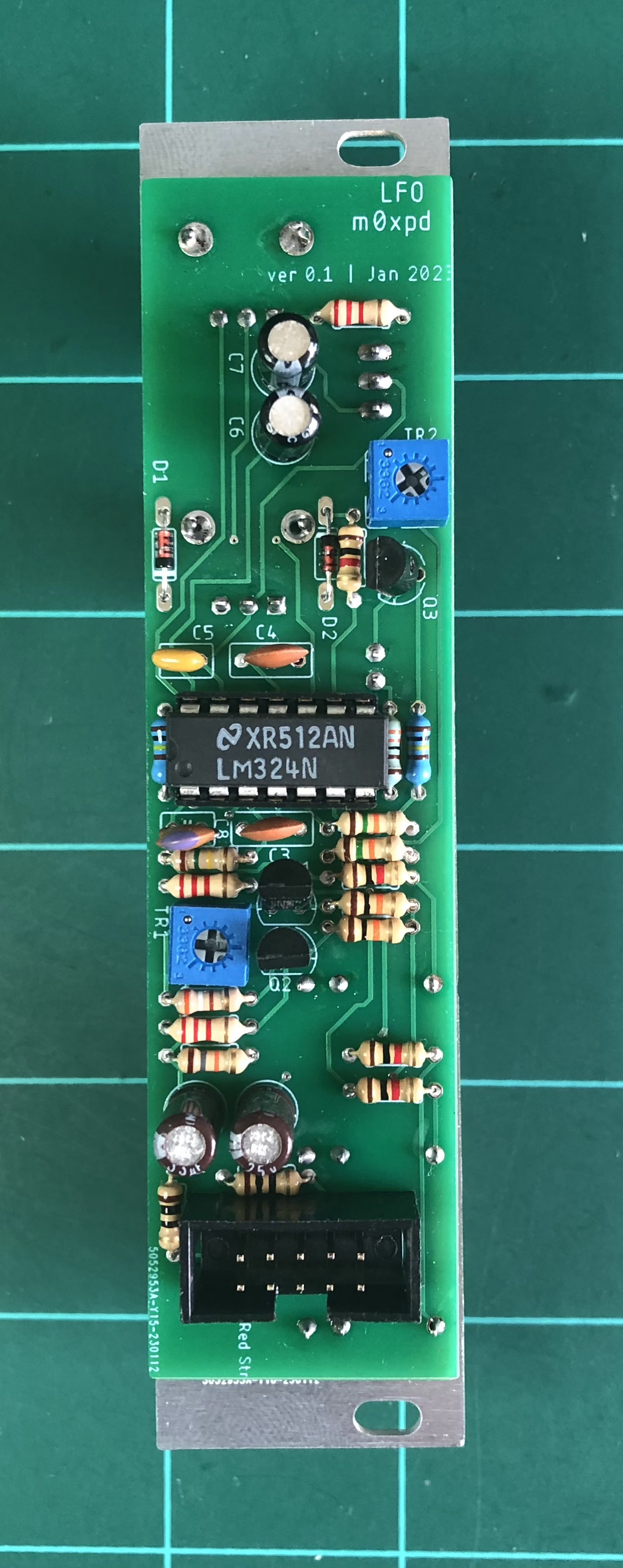
The second of my Eddy-inspired new builds is a Low Frequency Oscillator. 

My first LFO goes right back to the start of my synth adventure. It is a design by the late, great Ray Wilson, whose website 'Music From Outer Space' (MFOS) has been left up as a tribute to Ray's creativity and as a wonderful resource. My original LFO offered two oscillators with square or ramp outputs. 

When I decided (in January this year) to build a new LFO, I looked again at Eddy's site. Sure enough, there was a suggestion there for an LFO with 'variable skew' designed by Ken Stone. I was attracted by Eddy's words: 
"A simple LFO with pulsewave (with variable pulse width) and a seamless transition between a Ramp wave, Triangle wave and Sawtooth wave using one potmeter. With LED rate indicators and Speed and Shape controls." 
However, I couldn't help remembering something similar on the MFOS site.

Sure enough, there is a 'variable skew' design on MFOS which offers the additional benefit of a 'sinewave' output. That got me thinking.

I wanted a 'sinewave' output, because I like the idea of modulation sources without discontinuities (like the step-wise discontinuities in the squarewaves or the gradient discontinuities in the ramp, neither of which are really what we want when we're trying to make "whoosing" or "swirling" effects...). 

I decided to go with something closer to the MFOS design but, as a fully signed up cheapskate, I resented the idea of 'wasting' an LM13700 on the task of triangle to sinewave conversion, even though I have an embarrassing number of 13700s in 'stores'. Instead, I used the old differential pair ploy, now widely associated with Thomas Henry, familiar to  readers of Eddy's site

Here's my schematic:


Here's one of my new LFOs, seen from all important angles:


Once again, there's not a wire in sight. Oh and yes - you do see an LM324 there. I'm starting a one-man crusade against the indiscriminate use of TL074s everywhere. There are simpler alternatives which should be used, especially when the price of semiconductors (and everything else) is so crazy! I even got a bunch of TL084s (at a good price) and intend to remind the world that there may be times when we need the JFET input impedance, but don't need the last scintilla the TL07x offers over the TL08x. Perhaps I shouldn't say that in case it pushes up the price of TL084s!

Of course, the 'sinewave' is only a (poor man's approximation to a) sinewave when the shape control is centralised; at either extreme of travel the 'sine' output approaches what might best be described as a train of sigmoid functions, which is why I labelled the output "Curve" on the front panel.

Needless to say (again) everything works fine and it is a joy to have too many LFOs, rather than too few.

So - here are two modules, built according to my new design practice, standing on the shoulders of the original design work of Yves Usson and Ray Wilson and motivated (at least in part) by the words of blogger and inspiration Eddy Bergman.

73,
m0xpd